- 您现在的位置:买卖IC网 > Sheet目录480 > MTD6N15T4 (ON Semiconductor)MOSFET N-CH 150V 6A DPAK
�� �
�
�MTD6N15�
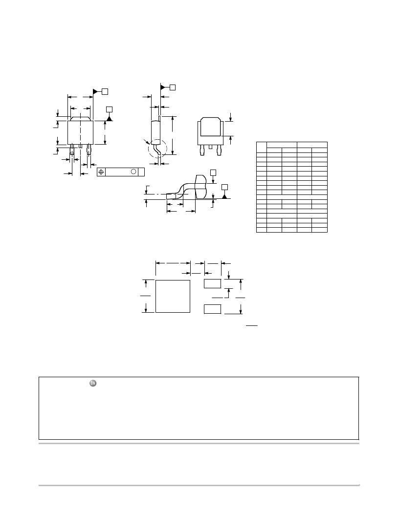
�PACKAGE� DIMENSIONS�
�DPAK� (SINGLE� GAUGE)�
�CASE� 369C�
�ISSUE� D�
�L3�
�1�
�E�
�b3�
�4�
�2�
�3�
�A�
�D�
�B�
�DETAIL� A�
�A�
�C�
�c2�
�H�
�Z�
�NOTES:�
�1.� DIMENSIONING� AND� TOLERANCING� PER� ASME�
�Y14.5M,� 1994.�
�2.� CONTROLLING� DIMENSION:� INCHES.�
�3.� THERMAL� PAD� CONTOUR� OPTIONAL� WITHIN� DI-�
�MENSIONS� b3,� L3� and� Z.�
�4.� DIMENSIONS� D� AND� E� DO� NOT� INCLUDE� MOLD�
�FLASH,� PROTRUSIONS,� OR� BURRS.� MOLD�
�FLASH,� PROTRUSIONS,� OR� GATE� BURRS� SHALL�
�NOT� EXCEED� 0.006� INCHES� PER� SIDE.�
�5.� DIMENSIONS� D� AND� E� ARE� DETERMINED� AT� THE�
�OUTERMOST� EXTREMES� OF� THE� PLASTIC� BODY.�
�6.� DATUMS� A� AND� B� ARE� DETERMINED� AT� DATUM�
�PLANE� H.�
�INCHES�
�MILLIMETERS�
�L4�
�b2�
�e�
�b�
�0.005� (0.13)�
�M�
�C�
�c�
�L2�
�GAUGE�
�PLANE�
�L�
�L1�
�DETAIL� A�
�ROTATED� 90� 5� CW�
�A1�
�H�
�C�
�SEATING�
�PLANE�
�DIM�
�A�
�A1�
�b�
�b2�
�b3�
�c�
�c2�
�D�
�E�
�e�
�H�
�L�
�L1�
�L2�
�L3�
�L4�
�MIN� MAX�
�0.086� 0.094�
�0.000� 0.005�
�0.025� 0.035�
�0.030� 0.045�
�0.180� 0.215�
�0.018� 0.024�
�0.018� 0.024�
�0.235� 0.245�
�0.250� 0.265�
�0.090� BSC�
�0.370� 0.410�
�0.055� 0.070�
�0.108� REF�
�0.020� BSC�
�0.035� 0.050�
�???� 0.040�
�MIN� MAX�
�2.18� 2.38�
�0.00� 0.13�
�0.63� 0.89�
�0.76� 1.14�
�4.57� 5.46�
�0.46� 0.61�
�0.46� 0.61�
�5.97� 6.22�
�6.35� 6.73�
�2.29� BSC�
�9.40� 10.41�
�1.40� 1.78�
�2.74� REF�
�0.51� BSC�
�0.89� 1.27�
�???� 1.01�
�Z�
�0.155�
�???�
�3.93�
�???�
�SOLDERING� FOOTPRINT*�
�STYLE� 2:�
�PIN� 1.� GATE�
�2.� DRAIN�
�3.� SOURCE�
�4.� DRAIN�
�6.20�
�3.00�
�0.244�
�2.58�
�0.102�
�0.118�
�5.80�
�0.228�
�1.60�
�0.063�
�6.17�
�0.243�
�SCALE� 3:1�
�mm�
�inches�
�*For� additional� information� on� our� Pb� ?� Free� strategy� and� soldering�
�details,� please� download� the� ON� Semiconductor� Soldering� and�
�Mounting� Techniques� Reference� Manual,� SOLDERRM/D.�
�ON� Semiconductor� and� are� registered� trademarks� of� Semiconductor� Components� Industries,� LLC� (SCILLC).� SCILLC� owns� the� rights� to� a� number� of� patents,� trademarks,�
�copyrights,� trade� secrets,� and� other� intellectual� property.� A� listing� of� SCILLC’s� product/patent� coverage� may� be� accessed� at� www.onsemi.com/site/pdf/Patent� ?� Marking.pdf.� SCILLC�
�reserves� the� right� to� make� changes� without� further� notice� to� any� products� herein.� SCILLC� makes� no� warranty,� representation� or� guarantee� regarding� the� suitability� of� its� products� for� any�
�particular� purpose,� nor� does� SCILLC� assume� any� liability� arising� out� of� the� application� or� use� of� any� product� or� circuit,� and� specifically� disclaims� any� and� all� liability,� including� without�
�limitation� special,� consequential� or� incidental� damages.� “Typical”� parameters� which� may� be� provided� in� SCILLC� data� sheets� and/or� specifications� can� and� do� vary� in� different� applications�
�and� actual� performance� may� vary� over� time.� All� operating� parameters,� including� “Typicals”� must� be� validated� for� each� customer� application� by� customer’s� technical� experts.� SCILLC�
�does� not� convey� any� license� under� its� patent� rights� nor� the� rights� of� others.� SCILLC� products� are� not� designed,� intended,� or� authorized� for� use� as� components� in� systems� intended� for�
�surgical� implant� into� the� body,� or� other� applications� intended� to� support� or� sustain� life,� or� for� any� other� application� in� which� the� failure� of� the� SCILLC� product� could� create� a� situation� where�
�personal� injury� or� death� may� occur.� Should� Buyer� purchase� or� use� SCILLC� products� for� any� such� unintended� or� unauthorized� application,� Buyer� shall� indemnify� and� hold� SCILLC� and�
�its� officers,� employees,� subsidiaries,� affiliates,� and� distributors� harmless� against� all� claims,� costs,� damages,� and� expenses,� and� reasonable� attorney� fees� arising� out� of,� directly� or� indirectly,�
�any� claim� of� personal� injury� or� death� associated� with� such� unintended� or� unauthorized� use,� even� if� such� claim� alleges� that� SCILLC� was� negligent� regarding� the� design� or� manufacture�
�of� the� part.� SCILLC� is� an� Equal� Opportunity/Affirmative� Action� Employer.� This� literature� is� subject� to� all� applicable� copyright� laws� and� is� not� for� resale� in� any� manner.�
�PUBLICATION� ORDERING� INFORMATION�
�LITERATURE� FULFILLMENT� :�
�Literature� Distribution� Center� for� ON� Semiconductor�
�P.O.� Box� 5163,� Denver,� Colorado� 80217� USA�
�Phone� :� 303� ?� 675� ?� 2175� or� 800� ?� 344� ?� 3860� Toll� Free� USA/Canada�
�Fax� :� 303� ?� 675� ?� 2176� or� 800� ?� 344� ?� 3867� Toll� Free� USA/Canada�
�Email� :� orderlit@onsemi.com�
�N.� American� Technical� Support� :� 800� ?� 282� ?� 9855� Toll� Free�
�USA/Canada�
�Europe,� Middle� East� and� Africa� Technical� Support:�
�Phone:� 421� 33� 790� 2910�
�Japan� Customer� Focus� Center�
�Phone:� 81� ?� 3� ?� 5817� ?� 1050�
�http://onsemi.com�
�6�
�ON� Semiconductor� Website� :� www.onsemi.com�
�Order� Literature� :� http://www.onsemi.com/orderlit�
�For� additional� information,� please� contact� your� local�
�Sales� Representative�
�MTD6N15/D�
�发布紧急采购,3分钟左右您将得到回复。
相关PDF资料
MTD6N20ET4
MOSFET N-CH 200V 6A DPAK
MTD6P10E
MOSFET P-CH 100V 6A DPAK
MTD8000N4-T
PHOTOTRANS 880NM DOME CLR TO-18
MTD8600N-T
PHOTOTRANS 880NM DOME CLR TO-18
MTD8600N4-T
PHOTOTRANS 880NM DOME CLR TO-18
MTD8600T-T
PHOTOTRANS 880NM FLAT CLR TO-18
MTD8600T4-T
PHOTOTRANS 880NM FLAT CLR TO-18
MTE1081C
INFRARED EMITTER 3MM 810NM
相关代理商/技术参数
MTD6N15T4G
功能描述:MOSFET NFET DPAK 150V 6A 300mOhm RoHS:否 制造商:STMicroelectronics 晶体管极性:N-Channel 汲极/源极击穿电压:650 V 闸/源击穿电压:25 V 漏极连续电流:130 A 电阻汲极/源极 RDS(导通):0.014 Ohms 配置:Single 最大工作温度: 安装风格:Through Hole 封装 / 箱体:Max247 封装:Tube
MTD6N15T4GV
功能描述:MOSFET Single N-Ch 150V 6A RoHS:否 制造商:STMicroelectronics 晶体管极性:N-Channel 汲极/源极击穿电压:650 V 闸/源击穿电压:25 V 漏极连续电流:130 A 电阻汲极/源极 RDS(导通):0.014 Ohms 配置:Single 最大工作温度: 安装风格:Through Hole 封装 / 箱体:Max247 封装:Tube
MTD6N20
制造商:ON Semiconductor 功能描述:MOSFET N D-PAK
MTD6N20E
制造商:Rochester Electronics LLC 功能描述:- Bulk 制造商:ON Semiconductor 功能描述:
MTD6N20E1
制造商:Rochester Electronics LLC 功能描述:- Bulk 制造商:ON Semiconductor 功能描述:
MTD6N20ET4
功能描述:MOSFET 200V 6A N-Channel RoHS:否 制造商:STMicroelectronics 晶体管极性:N-Channel 汲极/源极击穿电压:650 V 闸/源击穿电压:25 V 漏极连续电流:130 A 电阻汲极/源极 RDS(导通):0.014 Ohms 配置:Single 最大工作温度: 安装风格:Through Hole 封装 / 箱体:Max247 封装:Tube
MTD6N20ET4G
功能描述:MOSFET NFET DPAK 200V 6A 700mOhm RoHS:否 制造商:STMicroelectronics 晶体管极性:N-Channel 汲极/源极击穿电压:650 V 闸/源击穿电压:25 V 漏极连续电流:130 A 电阻汲极/源极 RDS(导通):0.014 Ohms 配置:Single 最大工作温度: 安装风格:Through Hole 封装 / 箱体:Max247 封装:Tube
MTD6N20ET5G
功能描述:MOSFET NFET DPAK 200V 6A 700MO RoHS:否 制造商:STMicroelectronics 晶体管极性:N-Channel 汲极/源极击穿电压:650 V 闸/源击穿电压:25 V 漏极连续电流:130 A 电阻汲极/源极 RDS(导通):0.014 Ohms 配置:Single 最大工作温度: 安装风格:Through Hole 封装 / 箱体:Max247 封装:Tube